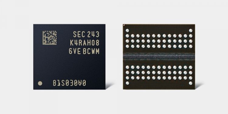
Samsung Electronics announced the development of its 16-gigabit (Gb) DDR5 DRAM using the industry’s first 12-nanometer (nm)-class process technology. Mass production of the new DRAM will start next year.
“Our 12nm-range DRAM will be a key enabler in driving market-wide adoption of DDR5 DRAM,” said Jooyoung Lee, Executive Vice President of DRAM Product & Technology at Samsung Electronics. “With exceptional performance and power efficiency, we expect our new DRAM to serve as the foundation for more sustainable operations in areas such as next-generation computing, data centers and AI-driven systems.”
Mass production set to start next year, Samsung said, “its new DRAM will advance next-generation computing, data centres and AI applications with industry-leading performance and greater power efficiency.”
Moreover, when combined with advanced, multi-layer extreme ultraviolet (EUV) lithography, the new DRAM features the industry’s highest die density, allowing for a 20% increase in wafer productivity.
Samsung claims that the new 12nm-class DRAM will help unlock speeds of up to 7.2 Gbps, which will help it process two 30GB UHD movies in just one second.
“We are thrilled to once again collaborate with Samsung, particularly on introducing DDR5 memory products that are optimised and validated on ‘Zen’ platforms,” Joe Macri, Senior VP, Corporate Fellow and Client, Compute and Graphics CTO at AMD said in a statement.
Consuming up to 23% less power than the previous DRAM, the 12nm-class DRAM will be an ideal solution for global IT companies pursuing more environment-friendly operations, said the company.
Also Read: IBM Collaborates with Japan’s Rapidus to Develop Advanced Chips


