SCREEN Semiconductor Solutions and IBM have made an agreement to develop cleaning processes for next-generation EUV lithography.
This agreement builds on their earlier work together to improve cleaning processes that support the current technology used in nanosheet devices.
In recent times, more companies are using EUV (Extreme Ultraviolet) lithography because there is a high demand for smaller and more advanced semiconductor products. The new High NA (High Numerical Aperture) EUV technology is especially critical for making chips smaller than 2 nanometers. In this advanced process, even tiny particles or scratches on the chip can cause problems, so cleaning is now more important than before. To solve these issues, IBM and SCREEN have agreed to focus on developing cleaning technologies specifically for High NA EUV.
This partnership combines IBM’s knowledge in semiconductor manufacturing with SCREEN’s advanced cleaning tools.
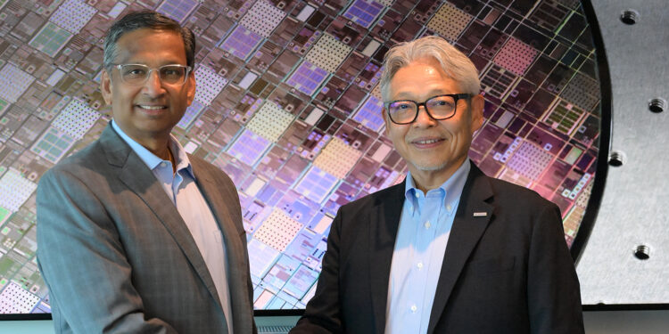
“High NA EUV technology is essential for developing smaller, more powerful semiconductors in the age of AI,” said Mukesh Khare, who is in charge of IBM Semiconductors. “We are excited to work more with SCREEN to make sure that we and our partners can take advantage of this new technology.”
Akihiko Okamoto, the President of SCREEN Semiconductor Solutions, also expressed the company’s enthusiasm about the partnership. “We are eager to strengthen our collaboration with IBM to create cleaning technologies that can meet the high requirements of High NA EUV lithography. By combining our expertise in precision cleaning with IBM’s comprehensive development process, we hope to deliver effective solutions that will help our customers develop sub-2nm devices.”
Through this agreement, IBM and SCREEN aim to speed up the development of cleaning technologies for advanced semiconductor manufacturing using High NA EUV lithography. They want to create solutions that provide the most benefits for device manufacturers.
Also Read: Why Even One Unpatched Device Can Be a Catastrophic Risk for Startups and SMBs